- “超级人类”:霍金担心基因改造会让自然人类灭绝
- 3m9002假的有用吗
- 磷酸钾(Potassium phosphate)「CAS号:7778532」 – 960 ...
- Ossila__迈可诺技术有限公司
- OS匀胶旋涂仪迈可诺技术有限公司
- Ossila狭缝涂布仪_华仪行(北京)科技有限公司
- Ossila狭缝挤出式旋涂机性能参数,报价/价格,图片
- 欧西拉/Ossila非真空旋涂仪精巧型功能应用性能参数,报价/价格,图片...
- Ossila/DMACDPS | 1477512325/250 mg/M2121A1_杯_耗材_其它...
- 杰出青年科学家奖
- ossila ossila批发价格、市场报价、厂家供应
- pce11 (pffbt4t2od) from £296.00


PFN is a conjugated polyelectrolyte used as an electron-interface in OPV devices to improve extraction efficiencies. Currently producing power conversion efficiencies of up to 7.1% at Ossila with further increases expected from additional optimisation and up to 9.2% reported in the literature [1-3].
Soluble in polar solvents such as water and methanol in the presence of small amounts of acetic acid.
General Information
| Full name | Poly [(9,9-bis(3"-(N,N-dimethylamino)propyl)-2,7-fluorene)-alt-2,7-(9,9–dioctylfluorene)] |
| Synonyms | PFN, PFN-DOF |
| Chemical formula | (C52H70N2)n |
| CAS number | 673474-74-3 |
Chemical Structure

Usage details
Inverted OPV devices were made using the architecture shown below with PFN (batch M221) as an electron-interface and PTB7:PC70BM in a 1:1.5 blend ratio (batches M211 and M113 respectively). Ossila"s pixelated cathode substrate pack (S173) provided the device components.
Glass / ITO (100 nm) / PFN (5.5 to 10 nm) / PTB7:PC70BM (90 nm) / MoOx (15 nm) / Al (100 nm)
The substrate cleaning and PFN spin-coating were performed under ambient conditions with all other steps performed in an N2 glove box until encapsulation had been completed (measurement performed under ambient conditions).
For generic details please see the fabrication guide and video. For specific details please see the condensed fabrication routine shown below. For information on our inexpensive Spin Coater for use with PFN please see our Spin Coater product page.
The active layer thickness, MoOx thickness, cathode metal (Ag or Al), PFN solution concentration, PFN drying/baking have not been fully optimised. As such, we expect further gains to be made with additional engineering work. However, for the devices made in this fabrication, a peak efficiency of 7.1% was achieved.

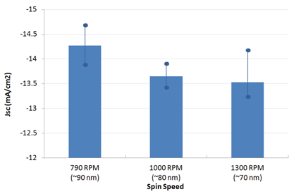
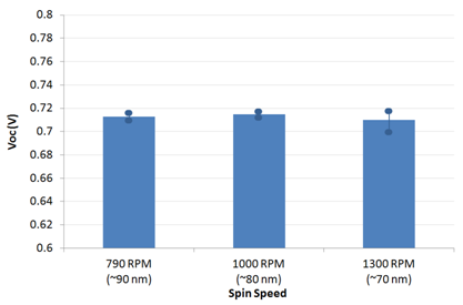
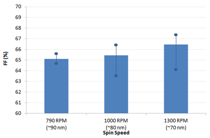

Note that some burn-in was observed (i.e. a small improvement in device performance after a few seconds under the solar simulator) and the variability of the devices is currently slightly higher than for other interlayers (average PCE of 6.7%). We expect the uniformity to improve with further improvements in PFN processing, in particular the optimisation of drying conditions to ensure that the acetic acid is fully removed prior to active layer deposition.
Fabrication Routine
The below fabrication routine was used to fabricate inverted solar cells with peak efficiency of 7.1%. Further gains are expected with further optimisation.
Substrates/Cleaning:
- Pixelated Cathode substrates (S173)
- 5 mins sonication in hot Hellmanex III (1 ml in beaker)
- 2x boiling water dump rinses
- 5 mins sonication in warm IPA
- 2x dump rinses
- 5 mins sonication in hot NaOH
- Dump rinse in boiling water
- Dump rinse in water
- Stored in DI water overnight and until use
PFN solution:
- Stock solution of acetic acid dissolved 1:9 in methanol to enable low concentration solutions to be made more easily.
- Acetic acid solution further dissolved to produce 2 μl/ml solution.
- PFN dissolved at 2 mg/ml in methanol with 2 μl/ml of acetic acid with stirbar at ambient temperature for 10 minutes
- Filtered through 0.45 µm PES filter
PFN Test Films
- PFN Test film initially spun at 500 rpm and gave 21-22 nm
- Second test film spun at 1000 rpm and gave 13-16 nm
- Thicknesses extrapolated for higher spin speeds
- It was noted that at low spin speeds 500 rpm to 2400 rpm there were significant crystallites present in the films - especially on the ITO. Extra filtration showed that this was not due to the solution and therefore most have been due to the drying process
Active Layer Solution
- Fresh stock solution of PTB7 made on at 10 mg/ml in CB and dissolved with stirbar for 1 hour (dissolves very easily)
- Mixed 1:1.5 with dry Ossila 95/5% C70 PCBM to make overall concentration of 25 mg/ml and dissolved with stirbar for 1 hour more
- 3% of diiodooctane (DIO) added to solution
- Filtered using 0.45 μm PTFE (hydrophobic) syringe filter
Active Layer Test Films
- Test film spun at 1000 rpm for 2 mins using unfiltered solution and thickness measure on Dektak. Note that films must be fully dry before performing Dektak measurements.
- 1000 rpm gave approximately 90 nm thickness.
Active layers
- Devices spun using 30 μl dynamic dispense (20 μl gave only moderate wetting/coverage)
- Spun for 2 mins
- Cathode wiped with CB
- Vacuum dried in glove box anti-chamber for 20 mins to remove residual DIO from films
Cathode Evaporation
- 15 nm of MoOx evaporated at 0.2 Å/s from fresh pellets at pressure <1e-6 mbar="" li="">
- 100 nm of Al evaporated at 1.5 Å/s at pressure <1e-6 mbar="" li="">
Annealing / Encapsulation
- No annealing performed
- Encapsulated as standard, using Ossila encapsulation epoxy (E132) and glass coverslips (C181) (30 mins in UV light box).
Measurements
- JV sweeps taken with Keithley 237 source-meter
- Illumination by Newport Oriel 9225-1000 solar simulator with 100 mW/cm2 AM1.5 output
- NREL certified silicon reference cell used to calibrate lamp output
- Lamp current: 7.9 A
- Solar output at start of testing: 0.995 suns at 25°C
- Solar output at end of testing: 1.00 suns at 25°C
- Electrochemically etched aperture mask was optically calibrated to 0.212 cm2
MSDS Documentation
 PFN MSDS sheet
Pricing
| Batch | Quantity | Price |
| M222 | 100 mg | £205.00 |
| M222 | 250 mg | £409.00 |
| M222 | 500 mg | £684.00 |
| M222 | 1 g | £1060.00 |
Literature and References
- Enhanced power-conversion efficiency in polymer solar cells using an inverted device structure, Z. He et al., Nature Photonics, 6, 591–595 (2012)
- Simultaneous Enhancement of Open-Circuit Voltage, Short-Circuit Current Density, and Fill Factor in Polymer Solar Cells, Z. He et al., Advanced Materials, 23, 4636–4643 (2011)
- Investigation of a Conjugated Polyelectrolyte Interlayer for Inverted Polymer:Fullerene Solar Cells, R. Xia et al., Advanced Energy Materials, (2013)
To the best of our knowledge the technical information provided here is accurate. However, Ossila assume no liability for the accuracy of this information. The values provided here are typical at the time of manufacture and may vary over time and from batch to batch.
专家支持 我们在这里为您提供帮助。我们的使命是为我们的产品提供最佳的技术支持,因此,如果您有任何疑问,请随时与我们联系。请更一般地享受这些指南,评论和对我们系统以及相关理论的概述。 视频指南和教程 使用PDMS进行2D材料的粘弹性转移 制作OLED和OPV太阳能电池:快速入门指南 空气钙钛矿设备 所有影片 书面指南和应用说明 旋涂 旋涂:膜厚指南 旋涂:难处理溶液指南 解决方案处理技术:比较 接触角:理论和测量指南 表面能指南 表面润湿的接触角测量 在不平坦表面上的接触角测量 薄层电阻:理论指南 四点探针测量指南 薄膜的薄层电阻测量 浸涂理论:膜厚 浸涂:缺陷故障排除指南 缝模涂布:理论,设计与应用 槽模涂布:缺陷故障排除指南 太阳能电池:理论与测量指南 IV曲线:测量指南 有机光伏:简介 有机光伏与第二代太阳能电池技术 有机光伏与第三代太阳能电池技术 OPV和OLED制作指南 大规模沉积有机太阳能电池 有机光伏绿色溶剂 钙钛矿和钙钛矿太阳能电池-简介 钙钛矿加工 FTO基板:将非图案化基板用于光伏设备 钙钛矿太阳能电池:增加稳定性和耐用性的方法 钙钛矿太阳能电池:退化的原因 钙钛矿太阳能电池:钝化技术 钙钛矿常见问题 二维材料简介 使用PDMS进行2D材料的粘弹性转移 二硫化钼 使用环保材料将氧化石墨烯还原为石墨烯 基于解决方案的OFET 什么是OLED? OLED测试指南 循环伏安法:电化学技术简介 文献评论:博士生凝聚 一名博士生凝结:OPV处理条件的影响 一名博士生凝视:ITIC及其衍生物成为OPV受体 一名博士生凝结:微调的ADA小分子受体 一名博士生凝结:影响OPV稳定性的因素 一名博士生凝结:三元有机太阳能电池简介 博士生凝聚:为新研究人员编写代码 系统概述 光伏基板概述 OLED基板(像素阳极)系统概述 低密度OFET制造系统概述和原理图 高密度OFET制造系统概述和原理图 解决方案处理的OFET基板系统概述 长通道OFET制作系统概述 Luminosyn™高纯聚合物